

Avalanche Technology’s Space Grade Ava-MRAM is engineered for exceptional write (program/erase) endurance. Traditional STT-MRAM stores its information within a Perpendicular Magnetic Tunnel Junction (pMTJ) whose underlying physics grant memory high cell endurance. Avalanche Ava-MRAM is built using a proprietary formulation for its pMTJ which offers unlimited write endurance. While many technologies claim to be “Space Grade,” true Space Grade requires that 5 objective criteria be met simultaneously. Space Grade technology must:
- Survive radiation without disruption
- Retain data for the life of a mission
- Endure unlimited writes
- Commit data instantly
- Prove real space heritage
This blog discusses in detail the third pillar of Space Grade, ENDURE, reflecting how the device’s write durability never becomes a limiting factor for real-time data collecting and processing in high radiation environments.
Memory Solutions Available Today
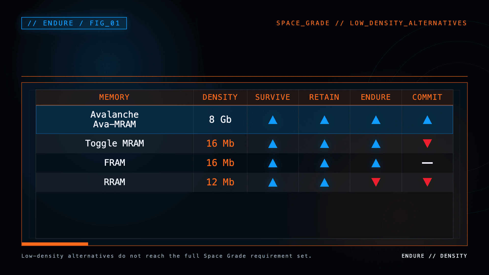
There are many considerations made when choosing the right memory for any application. Sustained exposure in extreme environments, such as space, poses additional difficulties for traditional memory devices. Consider the following memory types: FRAM, RRAM, and Toggle MRAM. All of these memories position themselves suitable for extreme industrial environments and space. Ferroelectric RAM, or FRAM, is a non-volatile memory technology that uses ferroelectric materials for durable storage with high endurance for read/write cycles. It offers fast write speeds, low power consumption, and strong resilience to radiation and extreme environments. Resistive RAM, or RRAM, is another non-volatile memory, built using a metal-insulator-metal structure, that promises similar features like low power operation and radiation resistance. In the future, it may offer high-density integrations, fast switching, and has a potential for scalable and low cost production. Toggle MRAM is a non-volatile technology that uses magnetic tunnel junctions with field-switched toggle-mode switching to store data via electron spin states. It provides SRAM-like speed, high endurance, and high reliability.
However, while these different memory technologies theoretically provide benefits for space applications, they have not been manufactured into real-world products at high densities. For FRAM, RRAM, and Toggle MRAM, their maximum densities available today are 16 Megabit, 12 Megabit, and 16 Megabit maximum. When comparing these memories to Avalanche’s Space Grade Ava-MRAM, the different densities are clear: Avalanche today offers up to an 8 Gigabit discrete product. The other memory technologies aren’t Space Grade because of their low densities.
Data Retention and Endurance: Measuring
JEDEC (formerly Joint Electron Device Engineering Council) is a global semiconductor industry standards organization. It develops and maintains technical standards for memory, storage, and other microelectronic components to ensure interoperability, reliability, and consistent testing methods across manufacturers. Accelerated testing is one such procedure outlined by JDEC. Because of the distinct physical structures of each memory technology, memory cell breakdown occurs in unique ways. Specifically, the failure mode of each memory cell type results from different stress vectors applied before or during a high-temperature bake.
Failure Modes
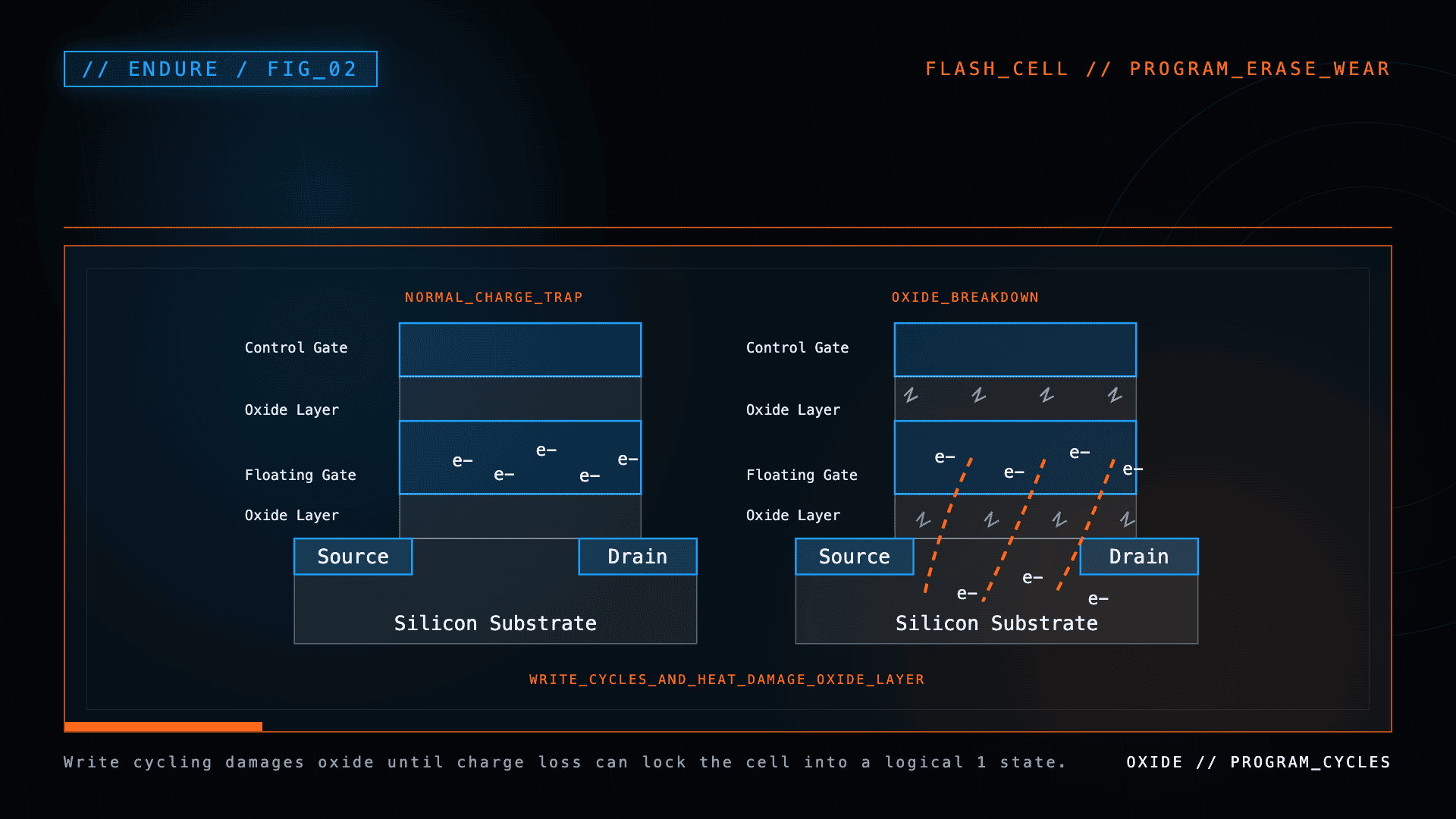
NAND and NOR flash memory function on a charge-trap based memory cell. A floating gate holding a charge is read as a “logical 0” and a floating gate not holding a charge is a “logical 1”. The thin oxide layer surrounding the floating gate breaks down over time and with the stress of write cycles, also called program cycles, on a cell. This damage to the oxide layer allows electrons to escape from the floating gate. The memory cell is dead when it functionally gets locked into a “logical 1” state. The number of times a cell is write-cycled dramatically affects the total lifespan of flash memory.
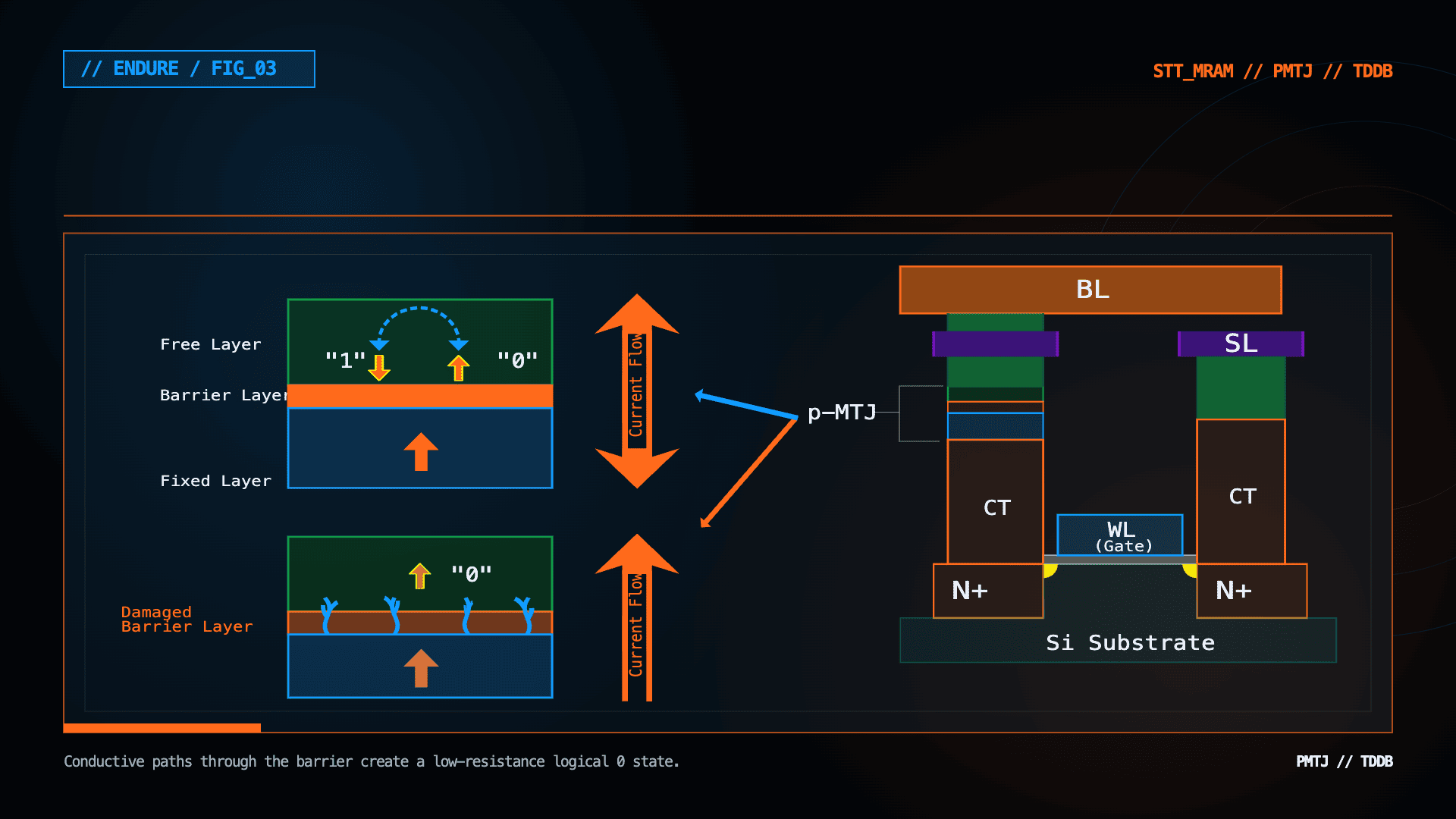
STT-MRAM cells operate on a different physical mechanism and consequently have a different failure mode. The base structure of the STT-MRAM cell is the Perpendicular Magnetic Tunnel Junction (pMTJ). This structure contains one tunnel barrier layer fixed between two ferromagnetic layers. The free layer can have its magnetic direction changed externally through thermally activated magnetic switching. This causes either high or low resistance within the tunnel which indicates a “logical 1” or “logical 0”, respectively. The mechanism of compromise for the pMTJ is Time-Dependent Dielectric Breakdown (TDDB). When the barrier oxide layer between the fixed and free layer breaks down, conductive paths can build through it and cause a low resistance path through the cell. Functionally, it locks the pMTJ into a “logical 0” state.
NAND and NOR vs STT-MRAM Endurance Testing
JEDEC device endurance validation uses the data gathered from accelerated testing and the use of an Arrhenius relationship to extrapolate lifespan at normal operating temperatures. When accelerated testing, a device is raised to an elevated temperature and held there for a determined period of time. Both flash memory and MRAM use accelerated testing for device endurance validation. The difference being that the activation energy term in Arrhenius equation does not apply to STT-MRAM devices. This is because NOR/NAND and MRAM have differences between their structure and failure modes.
For STT-MRAM devices, accelerated testing needs another stress factor added to induce TBBD. After selecting multiple groups of pMTJ devices, accelerated testing begins with an elevated temperature bake. During the bake, aggressive write-cycling with pulses of varying voltage are done for each group. The number of cycles are logged until pMTJ breakdown in each group and lifetime is extrapolated out to normal voltages.
The endurance testing of NAND and NOR flash devices differs from STT-MRAM. Because the Flash cell degrades with every single write (program/erase) operation, write-cycling precedes a data retention test. An example endurance test could have different blocks within a flash device be write-cycled at 0%, 1%, 10%, and 100% of the total rated write cycle endurance. The devices would also be validated at two different temperatures, room temperature and 85°C. If a device reaches its rated cycle endurance, and passes the data retention test, the device meets the validation standard.
Endurance Across Memory Types
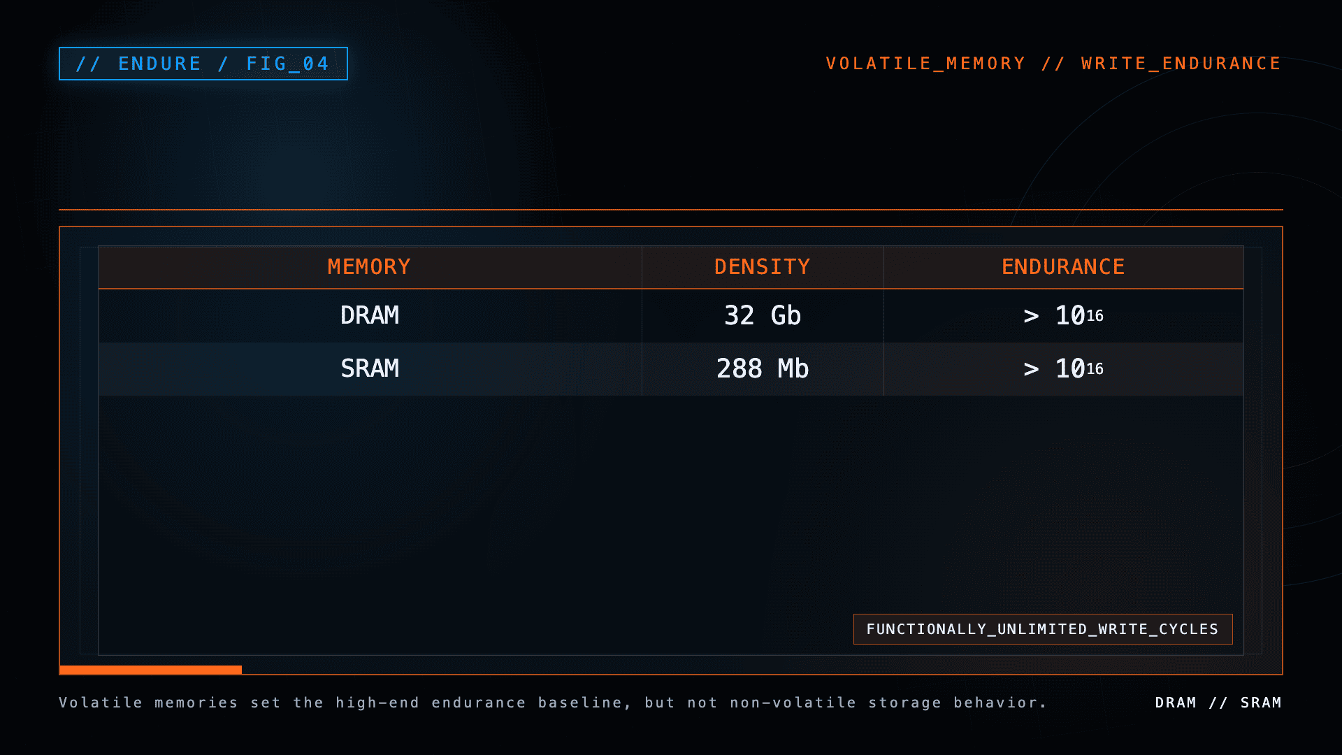
When strictly considering the endurance attributes of SRAM and DRAM, they have functionally unlimited endurance. The transistors of SRAM and the capacitors of DRAM do not break down in the way that flash memory cells do. Component malfunction occurs over a long period of time through mechanisms like TDDB.
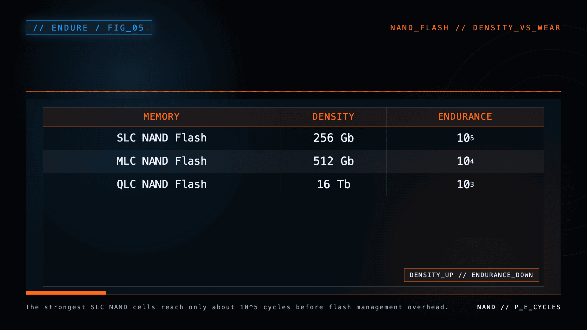
NAND flash provides the highest density of modern memory devices. Unfortunately, as NAND flash density increases, cell endurance dramatically decreases. Even among the common NAND technologies available, that is SLC, MLC, and QLC, only the lowest density SLC provides the best endurance figures. This is because higher density cells must store more bits per cell, which reduces the voltage margin between programmed states and increases susceptibility to wear. The most durable SLC NAND memory cells only have 50k – 100k write cycles under normal conditions before they break down.
The flash system overhead required to ensure NAND reliability introduces other drawbacks. Those will be discussed in a later section.
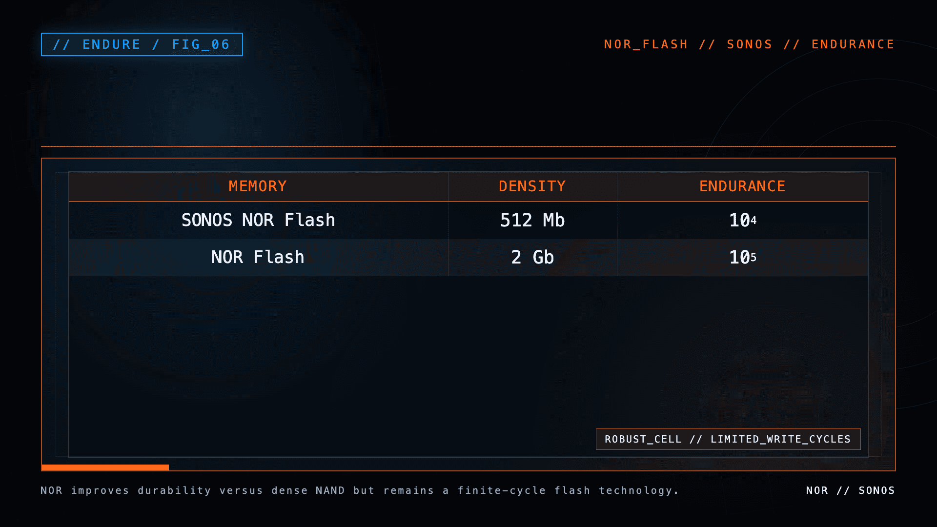
NOR flash has a more robust memory cell composition. Environmental factors like temperature change affect the NOR flash less than NAND flash. Typically, NOR flash is expected to endure ~100k write-cycles. Other formulations of NOR flash have been developed to increase its thermal durability and radiation resistance. SONOS NOR flash can manage around 10k write-cycles before cell breakdown occurs.
Flash Management
With limited write cycles, flash needs to be carefully managed to achieve reasonable lifespan. Reasonable being the key word here because it’s relative to other flash and not to other memory technologies. Flash memory is an erase-before-write memory. For NAND, the smallest unit of data that can be written is a page and the smallest unit of data that can be erased is a block, which is made up of multiple pages. The management issues with flash start with this disconnect between erase and write size. To write a single page, multiple pages need to be deleted and rewritten to a block. This write amplification needs to be carefully managed. The Write Amplification Factor (WAF) is the actual amount of data written into a flash device divided by the amount of data that was intended to be written into the device. Minimizing WAF is necessary as it decreases wear and preserves flash cells’ limited write cycles. Different strategies are used for this.
Simple wear leveling algorithms attempt to alleviate single block wear by spreading out writes to all blocks evenly. Superficially, this would seem like a sufficient wear reduction method. Unfortunately, this can inadvertently increase the total WAF because of the potential pairing of static (cold) data with dynamic (hot) data within a single block. Essentially, data that infrequently changes is being rewritten repeatedly because a section of its block contains frequently changing data. The unpairing of hot and cold data is an optimization challenge for other data management systems too. Regardless, for simple wear leveling purposes, more advanced data management schemes are required to reduce this source of write amplification.
Garbage collection attempts to reduce write amplification by lowering the rate of rewriting old stale data. The garbage collection process starts when a new write command comes in from the host and every block has been written to at least once. During garbage collection, a target block is first selected to be recycled. The garbage collection system then reads and holds onto the valid data, erases the block, and writes the new host-requested data alongside the old valid data that existed in the block. Old stale data is now deleted and will no longer be copied over on a new block write. The process of garbage collection causes write amplification because the total data written onto the device is more than the host requested to be written. It is an unavoidable source since there simply are no more empty blocks available. The benefit is that the removal of stale data reduces total extraneous writes and lowers overall device WAF.
A potential issue comes up with determining what is “valid data”. Stale data that is not properly marked for deletion can be carried over repeatedly by garbage collection. This severely increases the WAF. The flash translation layer (FTL), which translates logical block addresses into physical block addresses, can cause data remnants to be considered “good” even though they are a part of a file that the host has marked for deletion. The FTL is absolutely necessary for abstracting away the flash file system block management from the host. But, it can introduce communication errors between the host and device which result in stale data increasing the WAF.
Over provisioning helps with reducing write amplification. Over provisioning is additional capacity added to the storage drive that is not available to the host system. These extra reygions serve multiple purposes. For one, the contain the critical data, like firmware and the FTL. They also provide extra space for the garbage collection system and other management systems to operate in. Similar to the separation of hot and cold data, this scheme separates the flash filesystem data from the host data, which needs to be treated differently.
Overall, bad write amplification severely reduces total device life. Flash memory cells are limited by the total number of program-erase cycles they can withstand. Good write-amplification-reduction procedures are required to squeeze as much lifespan as possible out of delicate flash cells. However, this considerably increases the system overhead required to support flash memory devices.
Space Grade MRAM
Avalanche Technology’s Space Grade Ava-MRAM offerings withstand 1016 write cycles, which is functionally unlimited like SRAM and DRAM devices. Avalanches’ proprietary material composition enhances the intrinsically stable structure of the pMTJ. With the addition of endurance-optimized tuning, Avalanche provides unlimited write endurance that far exceeds traditional non-volatile memory technologies. These advancements remove the need for any wear leveling overhead and expose an SRAM-like logical structure to the host. Fundamentally, this eliminates memory device endurance as a design constraint in the demanding applications of aerospace, space, and defense.

Achieving Space Grade
For mission designers operating in the unforgiving conditions of space, memory device endurance cannot be an afterthought or a managed compromise. The Endure pillar of Avalanche’s Space Grade standard reflects a straightforward principle: memory hardware should never be the limiting factor in a mission’s capabilities. The structure of Avalanche Technology’s proprietary formulation of pMTJ provides extraordinary write-cycle endurance. It is a physics-defined, and craftfully engineered, advantage over other memory technologies available on the market today with exceptional data density.
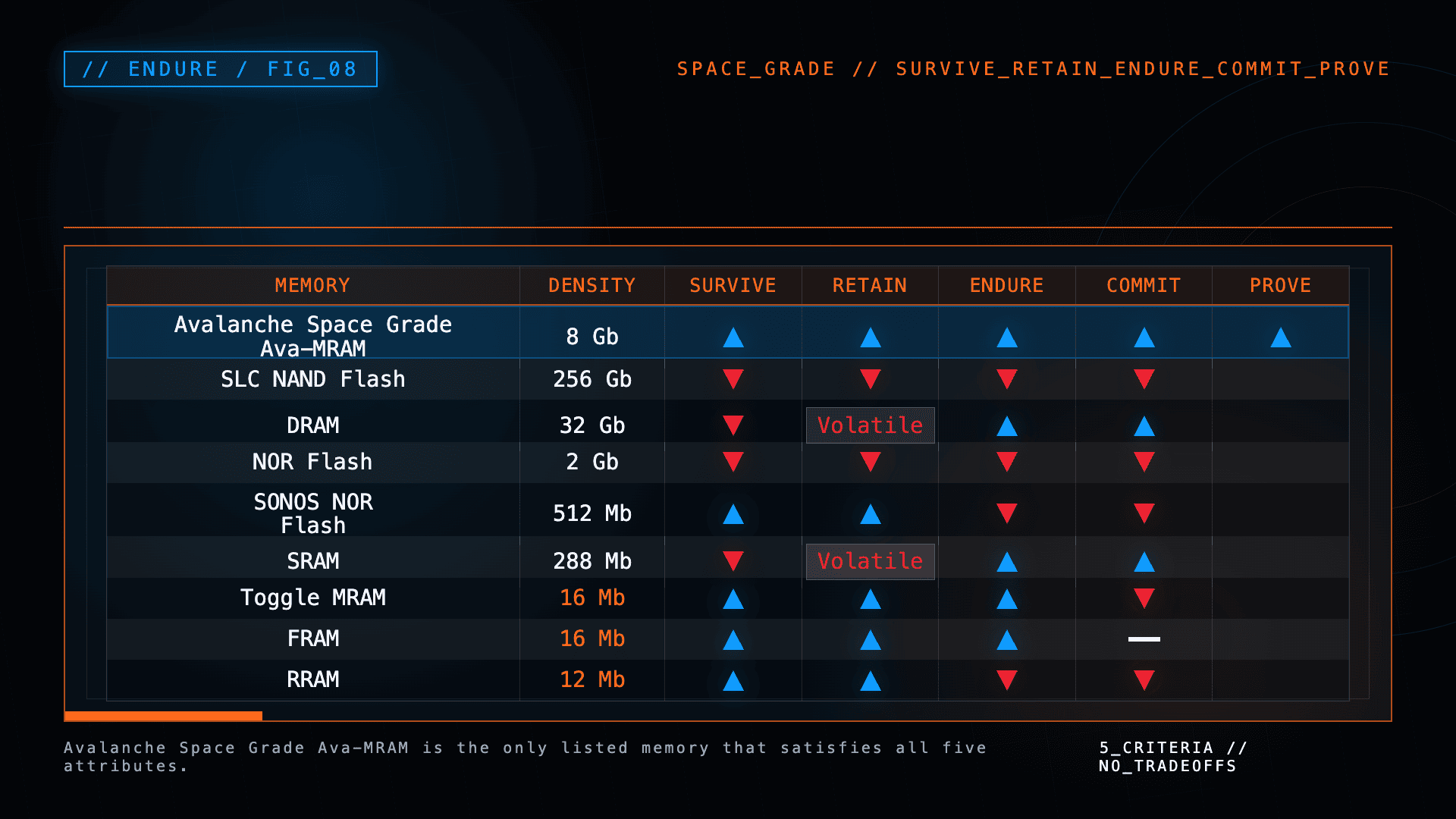
Ultimately, there is no one requirement of Space Grade that stands above the rest. Avalanche reaffirms its leadership as the only provider of true Space Grade memory, delivering solutions that meet all five non-negotiable criteria required for space missions: Survive, Retain, Endure, Commit, and Prove. Space Grade technology must survive radiation without disruption, retain data for the life of a mission, endure unlimited writes, commit data instantly, and prove real space heritage.
In space systems, a technology that survives radiation but loses data, wears out over time, delays data commitment, or lacks flight heritage is not Space Grade. Partial compliance leads to failure. Avalanche Space Grade Ava-MRAM uniquely delivers on all 5 criteria simultaneously, through radiation immunity, permanent data retention, unlimited endurance, deterministic nanosecond writes, and proven flight qualification, without tradeoffs.